PCB Design
Engineering
-
FPGA Design
Concept, Design, Development -
PCB Design
High Speed Digital
RF & Mixed Signal -
DSP
Simulation, Implementation -
Embedded Systems
Linux, Drivers, Scripting -
HMI Development
Qt, GUI, Usability
High Speed Digital
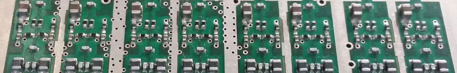
ARECS specializes in professionally designing PCB’s and developing them in fast turn-around times. Whether it is a simple two-layer board or a complex multi-layer PCB with auxiliaries*, we deliver high quality work with validated signal integrity you can rely on.
RF & Mixed Signal
ARECS has solid experience in RF & mixed signal design. We offer RF front end design services ranging from integration of standards based chipsets to full custom system development. In addition to complete products development capability, ARECS provides specialized design expertise for sub-systems**.
Mixed Signal design includes the integration of ADC’s and DACs with appropriate anti-alias filtering and matching to ensure the required performance. ADC/DAC interfaces range from simple SPI/I2C, parallel, LVDS, to multiple Gb/s JESD204B interfaces.
*FPGA, processor, DDR memory, high speed busses, high speed serial IO and special shielding requirements.
** Synthesizers, amplifiers, mixers, antennas and filters.

Know how
- BGA Layout
- Shielding
- Impedance Matching
- Trace Length Matching
- Signal Integrity
- DDR Layout
- High speed serial IO
- Board-to-Board Interconnect
- Design for Test + Manufacture